High side Mosfet swich design

Collapse
X
 
  • Time
  • Show
Clear All
new posts
  • AdrianM
    Member
    • Dec 2011
    • 39
    • UK

    #1

    High side Mosfet swich design

    I need to switch a 30Amp resistive DC load from a 5V microcontoller pin. This isn't PWM just occasional on/off.

    I'm familiar with the design considerations for high speed switching - rapidly getting charge in and out of the gate to minimise time spent in the linear region but in this application I'm pretty sure I can safely simplify the design a great deal because it's only used as a discrete on/off control.

    What I've come up with does seem uncomfortably slow so I thought I'd ask around in case I'm missing something!


    Q1 would actually be IPD50P04P413ATMA1 a 12mOhm P-Channel MOSFET, 50 A, 40 V. The total gate charge is less than 50nC so charging/discharging at around 5mA should take no more than 50nS x 1/0.005 = 10uS

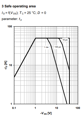
    This keeps it in the top right corner of the safe operating area:


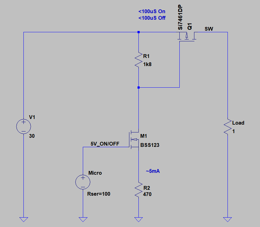
    The DC input could be as high as 30V so to limit the gate voltage low swing, the 470R source resistor makes M1 act like a constant current sink (its threshold being around 2.5V). R1 maintains around 10V across it until the supply drops below 12V

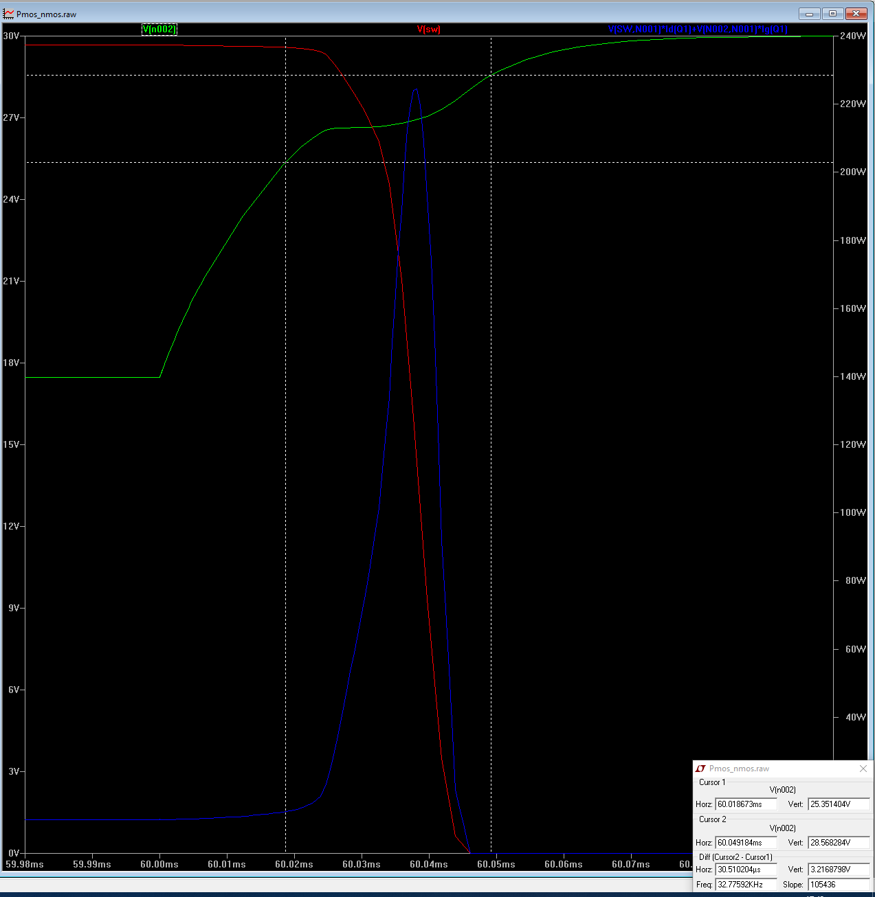
    LTspice sim of ~30uS switch-off for part with even higher gate charge (120nC) seems OK:


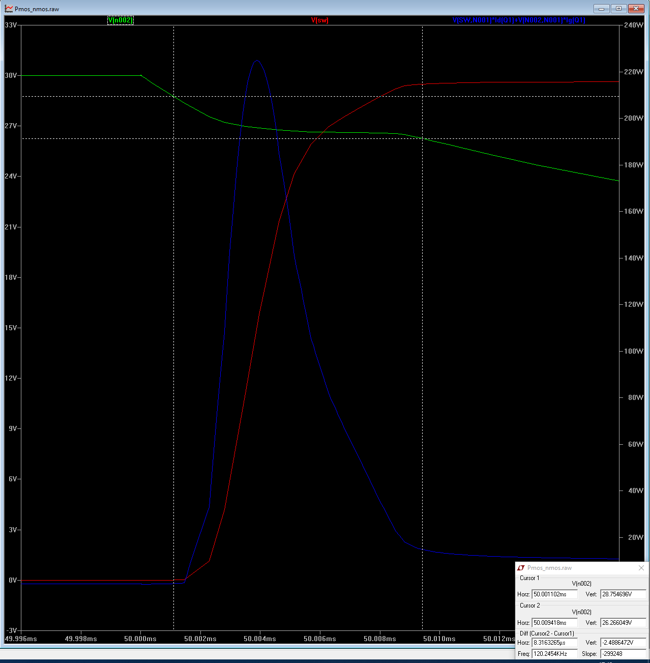
    Green is gate voltage, red ouptut voltage and blue power dissipation in Mosfet. Switch-on should be a bit sharper and it is at <10uS:


    Too good to be true? I'm so used to the pitfalls of Power PWM design that this simple application has me jittery
    Attached Files
  • eccerr0r
    Solder Sloth
    • Nov 2012
    • 8687
    • USA

    #2
    Re: High side Mosfet swich design

    Damn. I was looking for some ideas of high side switching and found this thread... grr PFET on V+ rail is low side switching. Not what I want. I want an IRF640 on the upper rail switching 150+ volts, controlled by a microcontroller. Need tens to hundreds of microsecond switching speeds - not insanely fast but not leisurely. Came up with a solution with no special components, but need to simulate it, and perhaps see some other ideas that don't involve custom driver chips...

    Anyway I don't understand R2 other than perhaps setting up a voltage divider. Having that there will kill performance of both transistors as it would limit how fast you can get the charge off of their gates.

    But do worry that the voltage divider is somewhat necessary due to exceeding the maximum gate voltage of Q1. Perhaps just moving R2 to the drain side of M1 will speed up performance and still maintain gate voltage limits.
    Last edited by eccerr0r; 06-02-2020, 10:23 PM.

    Comment

    • budm
      Badcaps Legend
      • Feb 2010
      • 40746
      • USA

      #3
      Re: High side Mosfet swich design

      1) Since M1 control the ON/OFF switch for Q1. How fast is M1 switching?
      2) "R1 maintains around 10V across it until the supply drops below 12V" If M1 switch is OFF, then I cannot see how you can maintain 10V across it.
      3) When M1 is OFF then the Q1 Gate will be discharged through R1so if you want to discharge it faster the put diode in parallel with R1, Anode on top end of R1.
      4) BTW, are you loading the SIM library with the actual spec of the component?
      https://cdn.badcaps-static.com/pdfs/...d97cb14944.pdf
      Attached Files
      Last edited by budm; 06-02-2020, 10:58 PM.
      Never stop learning
      Basic LCD TV and Monitor troubleshooting guides.
      http://www.badcaps.net/forum/showthr...956#post305956

      Voltage Regulator (LDO) testing:
      http://www.badcaps.net/forum/showthr...999#post300999

      Inverter testing using old CFL:
      http://www.badcaps.net/forum/showthr...er+testing+cfl

      Tear down pictures : Hit the ">" Show Albums and stories" on the left side
      http://s807.photobucket.com/user/budm/library/

      TV Factory reset codes listing:
      http://www.badcaps.net/forum/showthread.php?t=24809

      Comment

      • redwire
        Badcaps Legend
        • Dec 2010
        • 3900
        • Canada

        #4
        Re: High side Mosfet swich design

        OP's circuit, R2 is silly as it is limiting to 5mA and R1 is too low and a P-ch mosfet? not sure how the circuit even starts, it's prob. the substrate diode always on
        I always put in a gate zener, because you need to overdrive the gate to get good speed.
        Something else that works for driving high-side mosfets is photovoltaic opto-coupler, these have a tiny solar cell to make 10V for gate drive, at very low current though.

        Comment

        • eccerr0r
          Solder Sloth
          • Nov 2012
          • 8687
          • USA

          #5
          Re: High side Mosfet swich design

          Original circuit is fine with the P-channel with source to V+, that's how it's normally implemented, problem is that M1 won't saturate due to R2 - at first when the gate voltage is turned on, it works fine, but once it's on it will shut off because source voltage will increase... This is actually horrible and no wonder why it's working so poorly. So: short out R2, and if you don't want to dissipate as much power, put R2 on the drain lead so it will also reduce gate voltage of Q1 (though I've not looked at the data sheet for its maximum Vgs.)

          Alas I'm sorry, I necroed an old unanswered thread, but still wondering about my issue - finding other solutions to driving a high side N-channel mosfet switching 150V from a 5V signal with no custom ICs : just parts out of a 2-transistor switching power supply or at least that's the type of constraint I'm thinking about. So no photovoltaic isolators, though a photocoupler is acceptable.

          I suppose winding a transformer for the high side drive is also a possibility though I'd like to avoid transformers if possible, and if something comes up good with a transformer, I guess I can go with that - just no photovoltaics and no 'high side driver' chips...
          Last edited by eccerr0r; 06-03-2020, 01:15 AM.

          Comment

          • budm
            Badcaps Legend
            • Feb 2010
            • 40746
            • USA

            #6
            Re: High side Mosfet swich design

            Yep, R2 should be on the Drain of M1.
            Never stop learning
            Basic LCD TV and Monitor troubleshooting guides.
            http://www.badcaps.net/forum/showthr...956#post305956

            Voltage Regulator (LDO) testing:
            http://www.badcaps.net/forum/showthr...999#post300999

            Inverter testing using old CFL:
            http://www.badcaps.net/forum/showthr...er+testing+cfl

            Tear down pictures : Hit the ">" Show Albums and stories" on the left side
            http://s807.photobucket.com/user/budm/library/

            TV Factory reset codes listing:
            http://www.badcaps.net/forum/showthread.php?t=24809

            Comment

            • eccerr0r
              Solder Sloth
              • Nov 2012
              • 8687
              • USA

              #7
              Re: High side Mosfet swich design

              Okay, finally looked at data sheet but I shouldn't have bothered: Not only that R2 needs to be on the Drain of M1, it needs to be increased to 1KΩ if V1 is really 30V.

              and #@*%(#! can't get away from using p-channel MOSFETs or PNP transistors in my high side design (I was tempted to figure out how to incorporate a CD4069 but of course those have p-channel MOSFETs in them). I guess that's the way things go, but at least I don't need high power devices for the driver, just enough to pass maybe 1A for a very short amount of time...
              Last edited by eccerr0r; 06-03-2020, 08:56 AM.

              Comment

              • stj
                Great Sage 齊天大聖
                • Dec 2009
                • 30962
                • Albion

                #8
                Re: High side Mosfet swich design

                if you use a single "logic level" fet with a 2v gate voltage, the microcontroller can hard shift the gatepin from 5v to gnd - that will switch the fet much faster than using a pullup resistor or a current limiting resistor to ground.

                Comment

                • eccerr0r
                  Solder Sloth
                  • Nov 2012
                  • 8687
                  • USA

                  #9
                  Re: High side Mosfet swich design

                  But will that work well with a p-channel switch on the power rail that's well above 5V say 12V?

                  The second mosfet is there specifically for the level shifting needed to drive the p-channel. At least this is much simpler than a high side n-channel driver...

                  Comment

                  • stj
                    Great Sage 齊天大聖
                    • Dec 2009
                    • 30962
                    • Albion

                    #10
                    Re: High side Mosfet swich design

                    good question, not sure.

                    Comment

                    • budm
                      Badcaps Legend
                      • Feb 2010
                      • 40746
                      • USA

                      #11
                      Re: High side Mosfet swich design

                      Originally posted by eccerr0r
                      But will that work well with a p-channel switch on the power rail that's well above 5V say 12V?

                      The second mosfet is there specifically for the level shifting needed to drive the p-channel. At least this is much simpler than a high side n-channel driver...
                      The Gate Voltage of the P-CH has to be < the Source Voltage = to the Vth for full turn on of the MOSFET but it cannot be higher than the G-S breakdown Voltage. It is P-CH so we are pulling the Gate down not pulling up.
                      See the attached PDF in previous post on how it is done.
                      Never stop learning
                      Basic LCD TV and Monitor troubleshooting guides.
                      http://www.badcaps.net/forum/showthr...956#post305956

                      Voltage Regulator (LDO) testing:
                      http://www.badcaps.net/forum/showthr...999#post300999

                      Inverter testing using old CFL:
                      http://www.badcaps.net/forum/showthr...er+testing+cfl

                      Tear down pictures : Hit the ">" Show Albums and stories" on the left side
                      http://s807.photobucket.com/user/budm/library/

                      TV Factory reset codes listing:
                      http://www.badcaps.net/forum/showthread.php?t=24809

                      Comment

                      • eccerr0r
                        Solder Sloth
                        • Nov 2012
                        • 8687
                        • USA

                        #12
                        Re: High side Mosfet swich design

                        The answer is that the lower Vth devices do not help if the source voltage of the MOSFET is not referenced to ground, like the original post.

                        Any MOSFET on the high side has special problems to deal with. A P-channel with source at a fixed value (rail) is a bit easier to work with, at least the voltage is fixed.

                        Now my problem, a N-channel device on high side, the source voltage changes and likely above the voltage of microcontrollers, making it a much tougher problem. I've yet to find any good solutions other than requiring photovoltaic isolators, transformers, or special high side driver ICs. It would be interesting to figure out how to make a circuit that works like the high side driver IC.

                        Comment

                        Related Topics

                        Collapse

                        • Jane
                          How do you test MOSFET in laptops ?
                          by Jane
                          I tried to use this method:

                          Testing an N-channel MOSFET:

                          Step 1: Discharge the Gate (turn off the MOSFET)
                          Place the black probe (COM) on the Source (S) and the red probe on the Drain (D). The multimeter should show no continuity (high resistance or "OL" – open line).
                          Then, touch the black probe to the Source (S) and the red probe to the Gate (G). This discharges any stored charge in the Gate, turning the MOSFET off.

                          Step 2: Charge the Gate (turn on the MOSFET)
                          Now, place the red probe on the Gate (G) and the black probe on the
                          ...
                          09-27-2024, 03:31 AM
                        • zwerw3
                          High side mosfet of the power supply of the RTX2060 graphic chip burned out
                          by zwerw3
                          Hello. They brought a personal computer for repair in which the video card was GeForce RTX ™ 2060 WINDFORCE OC 6G (rev. 1.0). Graphics core power mosfet burned out.
                          Is there a chance to restore the site where the mosfet was? I started to grind the mosfet substrate with a dremel, which stuck to the board, but for now I stopped and decided to ask you for advice. I also noticed dark spots on the PCB near the video memory chips. Does this mean that the video memory is out of order? I cleaned the place where there was a burnout, a short circuit of 12 V was removed. On the coils on the power...
                          12-12-2022, 12:15 AM
                        • dougg3
                          Intel DX58SO high side VRM MOSFET keeps failing
                          by dougg3
                          Hi there,

                          I have an Intel DX58SO motherboard that failed last year. One of the high side VRM MOSFETs failed shorted, and it killed my i7 980 CPU. This motherboard has a 6-phase VRM. The parts used on this motherboard's VRM are:
                          • 6 x High side MOSFET: NTMFS4841NH
                          • 6 x Low side MOSFET: NTMFS4834N
                          • 6 x Driver: ADP3121JCPZ


                          It was easy to figure out where the short was, because the bad MOSFET's gate was shorted to the drain/source too. Once I removed it, all the shorts were gone on the motherboard, and I confirmed on the removed MOSFET itself that the gate/drain/source...
                          10-17-2021, 07:39 PM
                        • c_corr
                          Asus P4C800-E VRM issues
                          by c_corr
                          This board had the initial fault in VRM with high side Mosfet from PWM1 (phase 1) getting very hot. It also had the VRM caps quicly heating up in 10-15 seconds after power on.

                          This board uses mext ICs and Mosfets in VRM:
                          - ADP3180 PWM controller - in 3 phase mode
                          - ADP3418 as Modfet drivers
                          - High side Mosfets STD38NH02L (from ST)
                          - Low side Mosfets STD90NH02L

                          Some of the symptoms were very similar with the "Dead Asus P5P800-VM" in this forum.
                          I had the sawtooth voltage on Vcore too this was probably the cause of the Vcore caps...
                          02-08-2025, 11:59 PM
                        • IamPritesh
                          Asus GT531GT VCORE high side mosfet pad burnt
                          by IamPritesh
                          So I have this Asus GT531GT whose pad is burnt and it shows short to ground 0.8 even after removing all the connected mosfets and capacitors.

                          Image attached . The mosfet where the pad is burnt is PQH8102...
                          08-22-2022, 01:30 PM
                        • Loading...
                        • No more items.
                        Working...